How to power and talk to your CMOS sensors
Powering concepts, readout and data links.
Powering (general)
Modern particle tracking detectors are designed to combine large geometrical acceptance with micrometer-scale granularity, while simultaneously meeting stringent constraints on readout speed, power consumption, radiation tolerance, and material budget. In collider environments, the innermost tracking layers must operate close to the interaction point, where particle fluxes are highest and even small amounts of passive material degrade momentum and vertex resolution through multiple scattering.
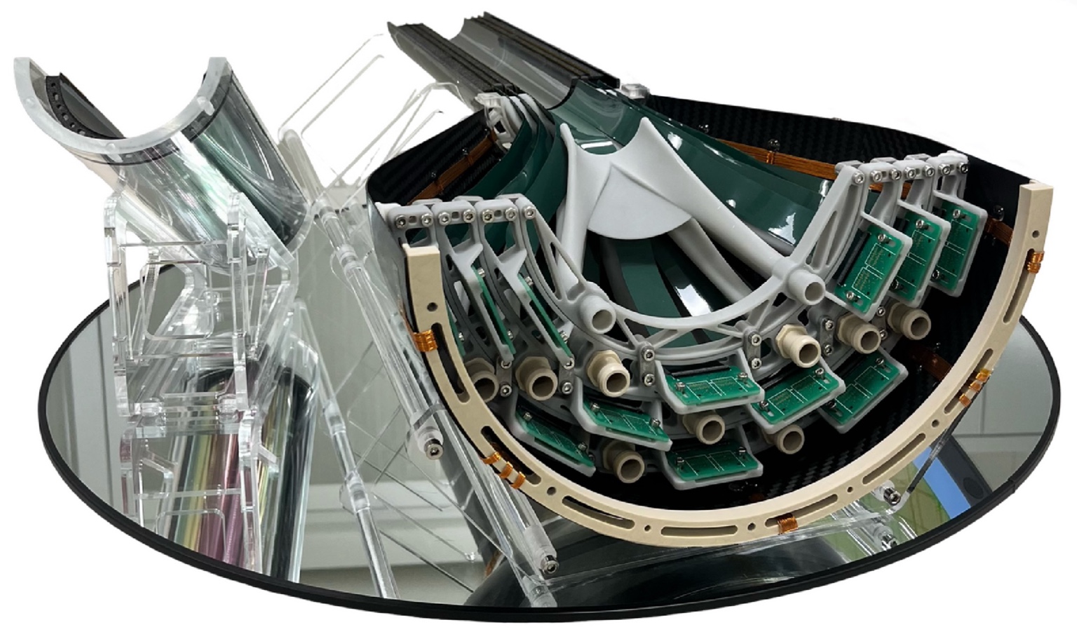
In practice, pixel chips cannot operate as standalone components. They must be mounted on a mechanical support, supplied with stable power, connected to (slow)-control and high-speed data links for communication, and thermally managed. These requirements are consolidated into a self-contained assembly known as a module. By standardizing this unit, large detector systems can be constructed through repetition of a well-characterized and highly-optimized building block.
This modular approach offers several advantages:
- Scalability to a large instrumented area of pixels
- Simplified assembly and quality control
- Ease of replacement and maintenance
- Parallelized production across institutes (or in industry)
- Segmentation: fault containment and localized performance loss (a malfunctioning unit reduces only a limited acceptance region rather than compromising the full stave or detector)
Within a module, individual chips are placed adjacent to each other with minimal dead space, separated only by a small nominal gap dictated by dicing tolerances and wire-bonding or interconnection constraints. The goal is to maximize the active area while maintaining electrical isolation and mechanical stability.
However, as detector areas increase, direct (point to point) powering and readout of every individual chip becomes impractical. The number of cables, connectors, and service lines would increase tremendeously (in a modern vertexer we have tens of billions of pixels = tens of billions of channels) and would introduce excessive material, complexity, and power losses. For this reason, modules serve not only as mechanical units, but also as electrical aggregation nodes:
- Power can be distributed locally (e.g. via serial powering or on-chip regulation).
- Data from multiple chips can be concentrated and transmitted through a reduced number of high-speed links.
- Control and clock signals can be shared across chips.
Modern pixel modules therefore integrate careful co-design of sensor and its associated front-end electronics (integrated in the same die for CMOS technology), power architecture, and data transmission scheme. Powering solutions must ensure stable operation under dynamic load conditions while minimizing resistive losses and material. Data transmission must provide high bandwidth, low bit error rate, and radiation tolerance — often over long, low-mass cables.
In this way, the module becomes the interface between the microscopic world of individual pixels and the macroscopic detector system, balancing performance, reliability, and material constraints.
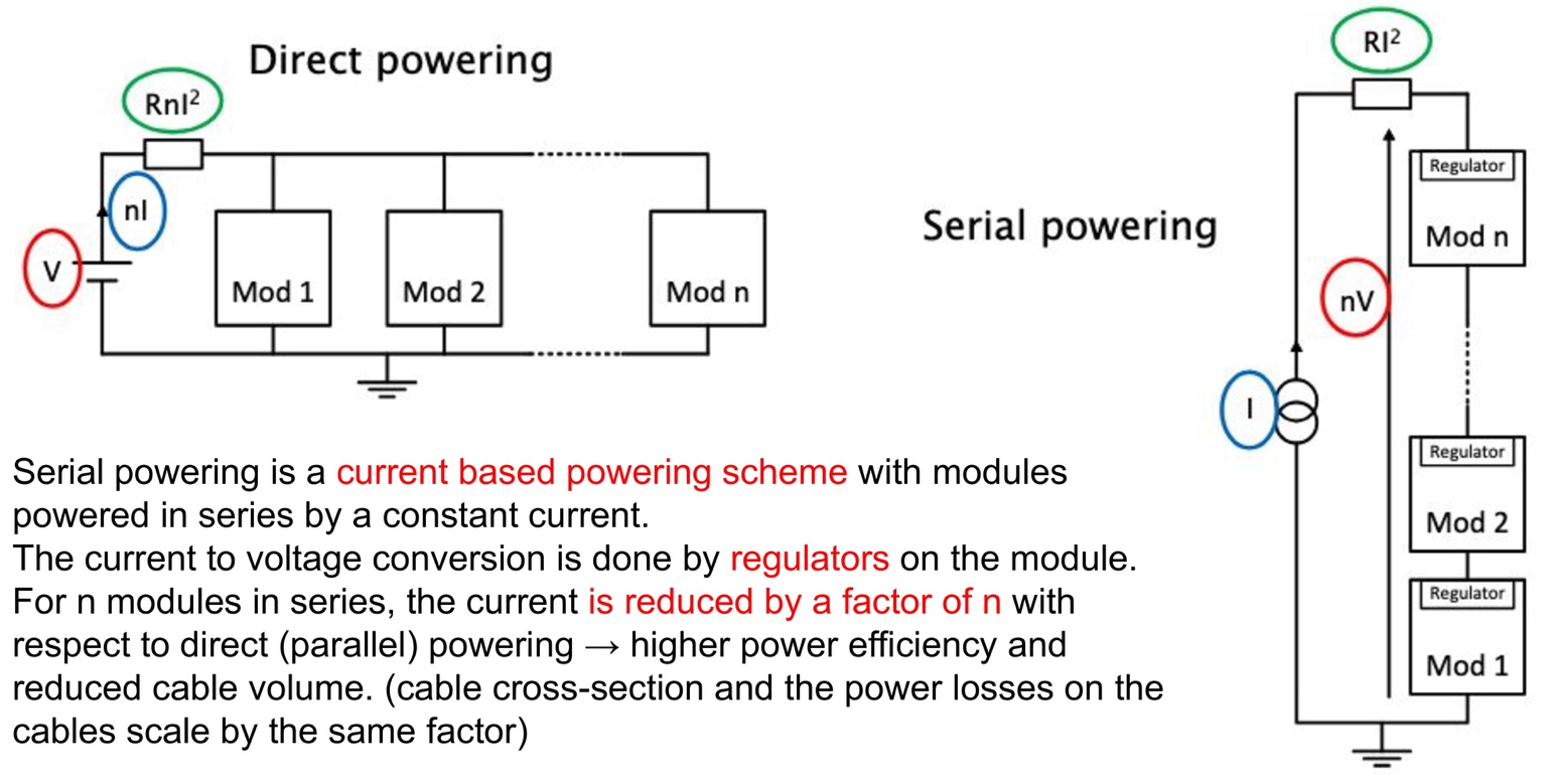
Several powering concepts are used in modern pixel detectors — most commonly parallel powering, DC–DC conversion, and serial powering — each addressing the challenges of voltage regulation, current distribution, cable material, and overall system efficiency in different ways.
The conventional scheme is parallel powering of modules with a constant voltage, enabling independent operation. For large-scale pixel detectors, however, low voltages and high currents over long cable runs can make cable losses comparable to (or larger than) the module power itself, while increasing service material.
Serial powering (general)
Serial Powering (SP) powers a chain of modules in series using a constant current. Only two power lines per chain are needed (instead of two per module). Voltages are generated by on-chip shunt and linear regulators.
For the ALICE 3 Outer Tracker (one of the big projects under the purview of the Pixel Platform), serial powering is the baseline option, driven by the detector scale (≈60 m2 of MAPS), long staves, strict material constraints, and air-cooling requirements that motivate low power densities.
Basic principle of serial powering
In a serially powered chain, a constant current source feeds multiple modules connected in series. Since the same current flows through all modules, each module must locally define its operating voltage. This is achieved using on-chip regulation stages.
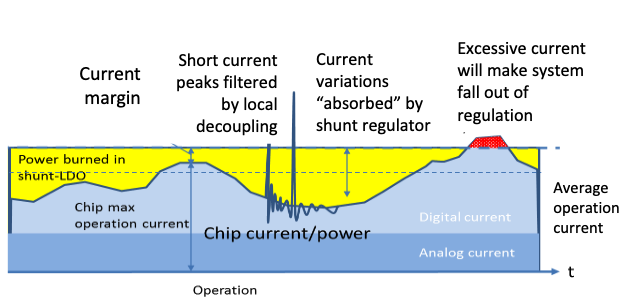
The key element enabling stable operation is the shunt regulator. A shunt behaves as a controlled current bypass: it diverts excess current away from the load in order to maintain a defined voltage across the module. In other words, while the chain current is fixed globally, the shunt ensures that local voltage variations caused by changing load conditions do not propagate through the chain.
Downstream of the shunt stage, linear regulators (LDOs) generate the precise internal supply rails required by the analog and digital circuitry. The shunt therefore provides coarse voltage stabilization at module level, while the LDOs ensure low-noise, tightly regulated local supplies.
Without a shunt element, variations in the current consumption of one module would directly affect the voltage distribution across the entire chain, potentially leading to instability. The shunt stage decouples modules electrically and guarantees controlled, predictable operation under dynamic load conditions.
Linear vs shunt LDO
In practice, both are needed. A linear regulator provides a stable, low-noise voltage for analog and digital domains, but it cannot sink current. A shunt regulator acts as a controlled current sink to burn off excess current and keep the chain current constant—protecting downstream modules when load current drops.
Slow Control and High-Speed Data Links
In addition to power delivery, pixel detector modules require communication links for configuration, monitoring, and data transmission. These links are typically divided into slow control and high-speed data paths, reflecting their fundamentally different bandwidth and latency requirements.
Slow control
Slow control interfaces are used for detector configuration, register programming, threshold tuning, monitoring of voltages and temperatures, and error reporting. The required bandwidth is modest, as commands and monitoring data are transmitted infrequently and involve small payloads.
These links are usually bidirectional, allowing commands to be sent to the detector while status information is returned. Typical implementations rely on robust, low-speed serial protocols optimized for reliability rather than bandwidth (e.g. LVDS).
High-speed data transmission
In contrast, the physics data path must handle the continuous stream of hit information produced by millions (or billions) of pixels. Collision environments with high interaction rates demand aggregate bandwidths in the multi-Gbit/s regime per module or stave.
High-speed links are therefore designed for maximum throughput and low bit error rate. They are typically unidirectional from detector to off-detector electronics, since the dominant traffic is physics data flowing outward. Differential signaling standards such as LVDS are commonly used to ensure signal integrity over low-mass cables (see on the right the ALICE ITS2 TDR chapter).
Implications for serial powering
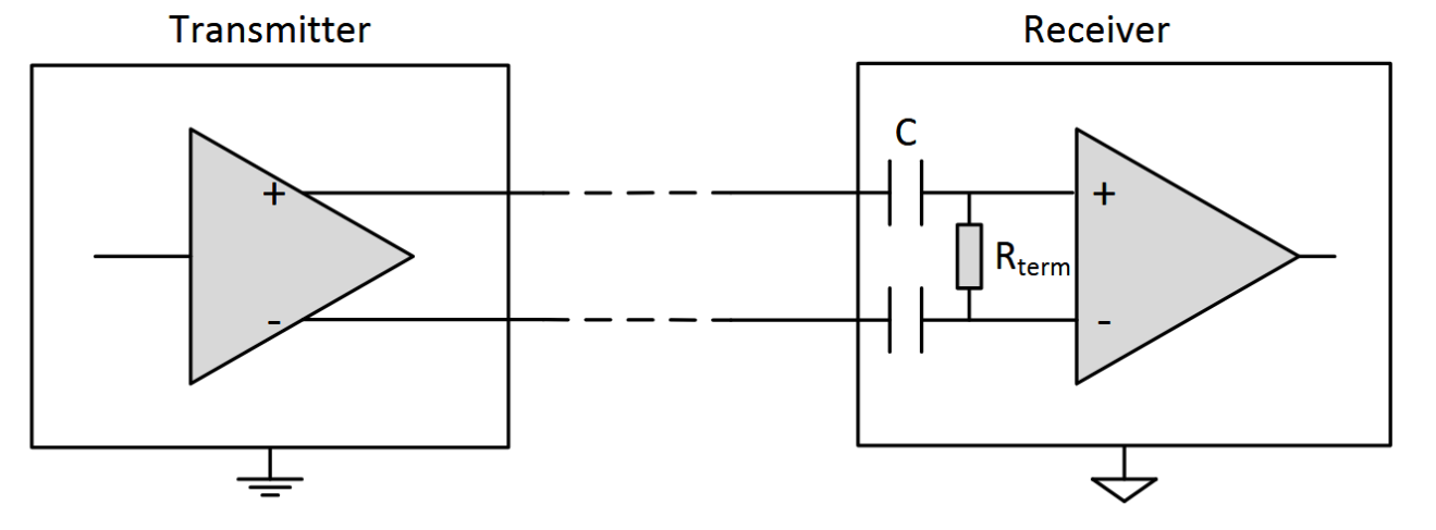
In serially powered chains, communication links must operate between modules that sit at different electrical potentials along the chain. This introduces additional design constraints. Data and control signals must either be AC-coupled or otherwise galvanically isolated to tolerate potential differences between neighboring modules. Without this, the LVDS common-mode voltage can shift outside receiver limits for upstream modules, degrading link integrity and risking damage.
Special care must be taken to ensure:
- Signal integrity across floating grounds
- Common-mode voltage compatibility
- Robust startup and fault behavior
- Minimal additional material from cabling
With AC-coupled termination, capacitors block DC components and the receiver sets the common-mode level. This requires a DC-balanced signal (e.g. clock) or an encoding (e.g. Manchester or 8b/10b) for command/data to ensure frequent transitions.
The co-design of powering and data transmission is therefore essential in serially powered systems, as grounding schemes, noise performance, and link stability are tightly coupled.
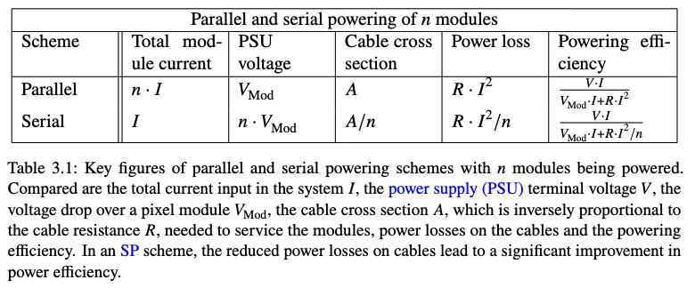
Parallel vs serial: key figures
Comparing total current, supply voltage, cable cross-section and losses shows why SP can significantly improve power efficiency and reduce service material—depending on how dominant services are in the overall power budget.
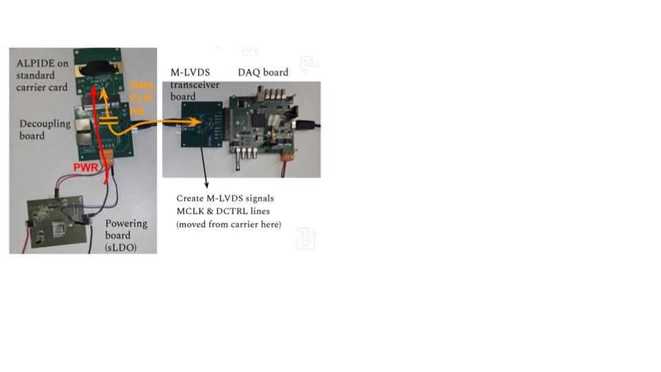
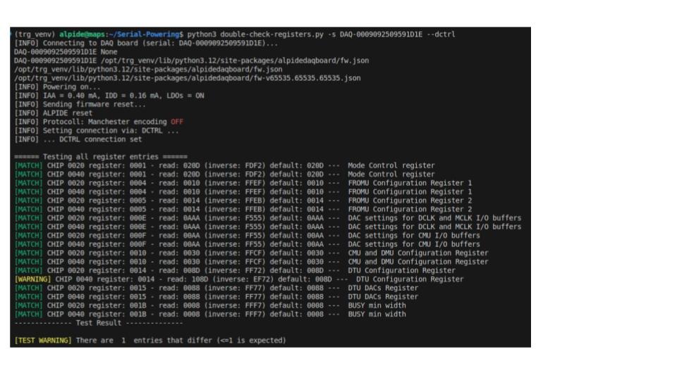
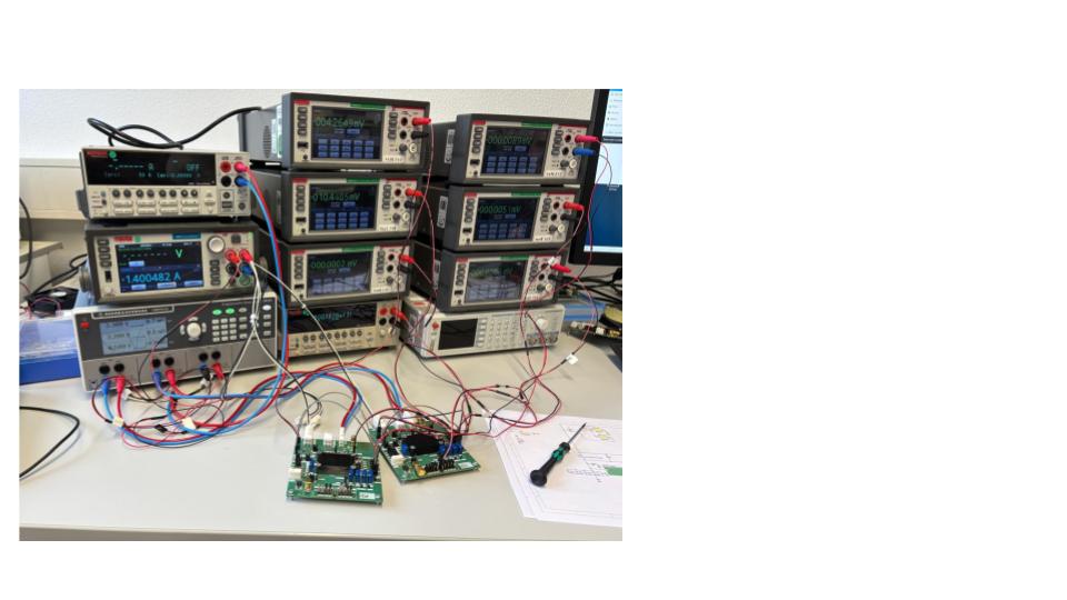
Tests at GSI and Local Expertise
Within the Pixel Platform at GSI, serial powering is not only studied conceptually, but validated experimentally through dedicated laboratory measurements.
Initial studies were performed using ALPIDE sensors powered in serial configuration with discrete shunt-LDO (sLDO) implementations (see: sLDO Heidelberg (V. Angelov, G. Fohner) ).
These setups allowed controlled investigation of startup behavior, load transients, noise coupling, and stability under realistic detector conditions.
The use of discrete regulator components provided flexibility in tuning operating points, studying failure scenarios, and validating grounding and AC-coupling schemes for high-speed data transmission in floating chains.
Building on these studies, the focus is now shifting towards 65 nm integrated sLDO solutions developed by Prof. Michael Karagounis (RD53b framework).
These regulators are representative of future large-scale pixel detector implementations, where integration density, radiation tolerance, and power efficiency are critical. The ongoing work at GSI aims to characterize their behavior in realistic serial powering chains and to evaluate their compatibility with long staves and low-material service routing.

This combination of discrete prototyping and advanced CMOS integration positions GSI as a site with hands-on expertise in both the conceptual and practical aspects of serial powering for next-generation pixel detectors.
Transition to 65 nm sLDO (RD53b)
Building on these studies, the focus is now shifting towards 65 nm integrated sLDO solutions developed by Prof. Michael Karagounis (RD53b framework).
These regulators are representative of future large-scale pixel detector implementations, where integration density, radiation tolerance, and power efficiency are critical. The ongoing work at GSI aims to characterize their behavior in realistic serial powering chains and to evaluate their compatibility with long staves and low-material service routing.
This combination of discrete prototyping and advanced CMOS integration positions GSI as a site with hands-on expertise in both the conceptual and practical aspects of serial powering for next-generation pixel detectors.
Add information
Add your information (Markdown) in the file:
content/page4.md
The text will automagically be converted to the right format.
Dr. Matthias Hamer (Bonn University) Detector Seminar – Efficient Powering of Inner Layer LHC Detector Electronics
Prof. Michael Karagounis (Fachhochschule Dortmund)
- Overview of powering architectures
- Serial powering concepts (shunt LDO)
- AC-coupled LVDS data transmission links
- Ongoing serial powering tests at GSI